
How do you integrate components into a printed circuit prototype?
integrate components into a printed circuit prototype
When turning your innovative electronic design into a physical printed circuit prototype, it is critical to integrate components correctly. Getting this right ensures the final product functions as intended and provides the best possible performance. To help with this, there are a few basic steps that can be followed, such as creating a schematic and ensuring it is linked to the PCB, defining the board and layer stack, deciding where to insert drill holes (mounting and vias), routing your traces and finally verifying your circuit board layout by running a design rule check (DRC).
A schematic still remains a vital part of the circuit design process even though manufacturers rely primarily on Gerber files and drill files for fabrication. This is because the schematic allows for clear communication between internal teams and external manufacturers, resulting in smoother collaboration and reducing mistakes that could result in costly rework and malfunctioning products.
One of the most important things to keep in mind when designing a schematic for a printed circuit prototype is separating different functional areas such as digital, analog, RF and power. This is because overlapping signals can cause interference and lead to poor performance. It is also recommended that high-speed signals be grouped together and kept at a short distance from each other to simplify the routing of these traces.
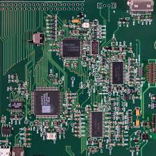
How do you integrate components into a printed circuit prototype?
Another important consideration is ensuring that all ICs are oriented in the same direction. This helps streamline the assembly process by allowing pick and place machines to easily locate their locations. It is recommended that polarized components such as diodes and capacitors are oriented with their positive terminals facing the silkscreen to further simplify the process.
It is also important to consider the amount of heat generated by a particular component. To avoid overheating, these hottest components should be placed near the center of the board so that they are closer to the surface and can dissipate their heat quickly. In addition, it is helpful to incorporate thermal sinks or other devices that improve heat dissipation.
In order to reduce confusion during the manufacturing process, it is also a good idea to use network labels when connecting individual ICs on a single page. This makes it easier for technicians to identify the connection and can eliminate the need to manually draw numerous connections between ICs. This will also allow the technician to quickly identify any ICs with missing or mismatched pinouts.
Lastly, when the PCB is drilled, it is important to create unique drill files for plated through-holes and non-plated through-holes. This will prevent mistakes during the manufacturing process and ensure that all holes are properly sized and aligned.
By following these simple steps, you can be confident that your finished circuit board will function as intended and provide the best possible performance. However, it is important to remember that it may take a few iterations before your final product works as you imagined. By being patient and utilizing the right resources, you can ensure that your prototype will perform as needed.