
How Do Micro Vias Impact Signal Skew?
Micro Vias Impact Signal Skew
As electronic products and components become smaller and more complex, it becomes a challenge to maintain signal integrity as the size of the conductive pathway increases. Micro vias are one way to increase density while ensuring the reliability of signals. However, as they continue to be implemented in PCBs, it is important to understand how micro vias impact signal skew and the potential for failure.
Signal skew is an undesirable effect of a circuit board that occurs when the electrical signal travels through different mediums such as PCB traces and interconnects. This distortion can lead to EMI (Electromagnetic Interference) issues that can reduce signal strength and cause the device to malfunction.
To address these problems, engineers can use micro vias that are filled with conductive epoxy or copper wrap plating to improve the quality of the signal and reduce EMI. These structures are small holes that can connect all layers of a printed circuit board (PCB) through which signal can flow. These microvias are commonly used in high-speed digital and RF applications that require a high level of signal transmission.
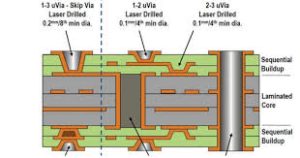
How Do Micro Vias Impact Signal Skew?
These small holes are difficult to manufacture as they must be drilled through the various layers of the PCB. This is typically done with a laser and requires careful manipulation of the drill’s settings to ensure that the hole has the correct shape and size. In addition, the drilling process can induce vibration that can create defects in the hole.
Once a microvia is drilled, the manufacturer fills it with pure copper or an epoxy + copper resin to ensure that the hole is properly connected to the other layers of the PCB. The manufacturer then uses a pulsed plating process to ensure that the copper is evenly distributed throughout the body of the microvia and eliminates any voids. A common problem with plated microvias is that the copper concentrates more on the top surface of the structure and less on the bottom, which can result in weak connections between the pad and the conductor.
Compared to plated through holes, microvias offer an advantage in that they can be designed to be either stacked or staggered. Staggered microvias allow designers to move the drilling position away from overcrowded areas of a plane and onto more unused spaces. This helps to improve power and ground plane performance and reduce EMI issues related to choke points.
As technology advances, it is likely that microvias will continue to be a popular solution for improving the design of electronic devices. To ensure that they are reliable, it is important to understand how the features influence signal skew and how to mitigate these effects. It is also critical to design the underlying components and the overall PCB with a sufficient level of redundancy to prevent microvia failures. To do this, engineers need to consider a number of factors including the geometry parameters of the PCB, fabrication process variables and stress and strain calculations in the microvias.